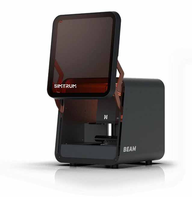
Maskless Lithography UV Laser Writer
| Compare |
Model |
|
Drawings & Specs |
Availability |
Reference Price
(USD) |
|
|
|
 |
LL-LW-405-4-0.8
Repeatability: 0.1 μm ,Stage Travel: 4"", 5"" compatible, Laser Wavelength: 405 nm (365/385 nm optional) ,Default Configuration: 20x. (0.8 μm, 15 mm²/min) ,Grayscale: 8-bit, 2K DMD resolution, Delivered with high performance laptop
|
|
6-10 Weeks |
Request for quote |
|
|
|
|
LL-LW-405-6-0.8
Repeatability: 0.1 μm ,Stage Travel: 6"" (8"" optional) ,Laser Wavelength: 405 nm (365/385 nm optional) ,Default Configuration: 20x. (0.8 μm, 15 mm²/min), Grayscale: 8-bit, 2K DMD resolution ,Delivered with high performance laptop
|
|
6-10 Weeks |
Request for quote |
|
|
|
|
LL-LW-405-4-1.5
Repeatability: 0.1 μm, Stage Travel: 4"" ,Laser Wavelength: 405 nm (365/385 nm optional) ,Default Configuration: 10x. (1.5 μm, 60 mm²/min) ,Grayscale: 8-bit, 2K DMD resolution ,Delivered with high performance laptop
|
|
6-10 Weeks |
Request for quote |
|
|
|
|
LL-LW-405-6-0.8-Upgrade
Repeatability: 0.1 μm ,Stage Travel: 8"" ,Laser Wavelength: 405 nm (365/385 nm optional) ,Default Configuration: 20x. (0.8 μm, 15 mm²/min), Grayscale: 8-bit, 2K DMD resolution, Delivered with high performance laptop
|
|
6-10 Weeks |
Request for quote |
|
LL-LW-Upgrade - Parameter
LL-LW-405-6-0.8-Upgrade - Parameter
LL-LW-405-4-1.5 - Parameter
LL-LW-405-6-0.8 - Parameter
LL-LW-405-4-0.8 - Parameter
LL-LW-405-6-0.8-Upgrade - Download
LL-LW-405-4-1.5 - Download
LL-LW-405-6-0.8 - Download
LL-LW-405-4-0.8 - Download
Accessories
| Compare |
Model |
|
Drawings & Specs |
Availability |
Reference Price
(USD) |
|
|
|
|
LL-LW-Upgrade
Dual Light Source: 405 nm+365 nm (Software selectable) ,Grayscale: 16-bit, 3K DMD resolution
|
|
6-10 Weeks |
Request for quote |
|
|
|
|
LL-LW-2.5
Linewidth: 6 μm
|
|
6-10 Weeks |
Request for quote |
|
|
|
|
LL-LW-5
Linewidth: 3 μm ,Patterning Speed: 200 mm2/min
|
|
6-10 Weeks |
Request for quote |
|
|
|
|
LL-LW-10
Linewidth: 1.5 μm ,Patterning Speed: 60 mm2/min
|
|
6-10 Weeks |
Request for quote |
|
|
|
|
LL-LW-20
Linewidth: 0.8 μm, Patterning Speed: 15 mm2/min
|
|
6-10 Weeks |
Request for quote |
|
|
|
|
LL-LW-50
Linewidth: 0.5 μm ,Patterning Speed: 3 mm2/min
|
|
6-10 Weeks |
Request for quote |
|
|
|
|
LL-LW-BSA
Only for LL-LW-405-6-0.8 ,Enables two-point alignment ,Alignment accuracy: < 2 um, Please confirm microscope placement before placing order
|
|
6-10 Weeks |
Request for quote |
|
|
|
|
LL-LW-Vacuum
Perforated sample stage to allow for vacuum-based workholding, Vacuum pump not included
|
|
6-10 Weeks |
Request for quote |
|