| Introduction
Nanoimprint and Wafer Level Optics (WLO) manufacturing involve master fabrication and replication of custom-designed lenses. Multiple cavities of miniaturized lenses can be made and populated closely across an entire wafer master. These are some of the most reliable processes for high volume manufacturing of micro & nano optics.
We has developed complete and broad base know-how / technology that paves the way for scalable, high-volume production of 500K-1.0M units per day demand. Both nanoimprint and WLO techniques can be leveraged upon to make highly precise, solder-compatible optics in a cost-efficient way. Optical features can range in size from 150nm to 100s of microns in sizes using a multitude of equipment and processes.
These techniques use materials that are commonly found in the market, ensuring good cost competitiveness in comparison to conventional high volume production techniques that is inadequate for small form-factor optical components.
| 
Product Brochure Link: 
Contact us at info@simtrum.com for customized service |
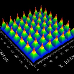
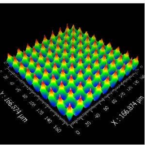
Nanofabrication Capabilities ● Mater Fabrication of Nano-Structures ● 3D Print Micro- & Nano-scale Prototypes ● Scalable Nanoimprint: 6" or 8" Wafer Level Optics ● Extensive Design form Factors: Spheres, Aspheres, Arrays, Gratings, Fresnels and other Diffractive Optical Elements (DOE). | 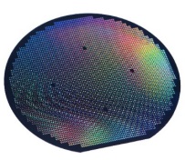
Wafer Level Optics (WLO)
|
In-house Technologies & Facilities
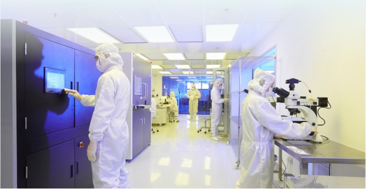
● 2-Photon-Polymerization (2PP) Printing Machines ● Direct Laser Writing (DWL) Machine ● Customized Wafer Level Optics (WLO) ● Scanning Electron Microscopy (SEM-EDX) ● Class 1K, 10K and 100K Cleanrooms
| 
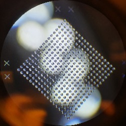
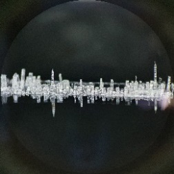
Grating 3D Printed via 2PP |
Established Nanofab Materials
● 2PP & DWL: Photoresists ● Monolithic Nanoimprint: Epoxy, Acrylate, etc. ● Hybrid Nanoimprint: Epoxy / Acrylate on Glass / Silicon / Polymeric Substrates.
| 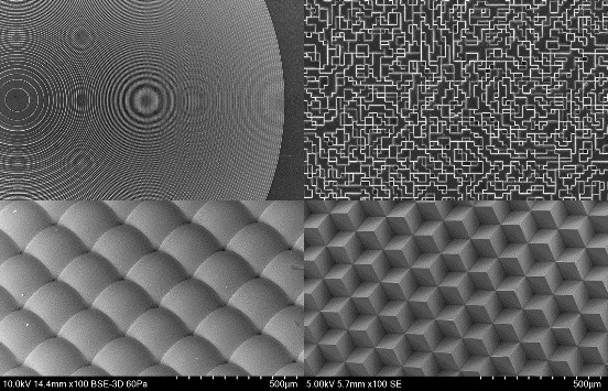
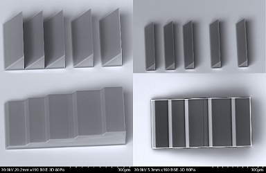
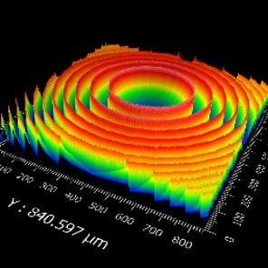
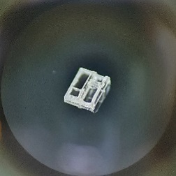
Nanoimprint Structures: Micro-fresnels, DOE, LEns Array & Corner Cubes |
| Optical Design & Simulation Software |
|
|
|
|
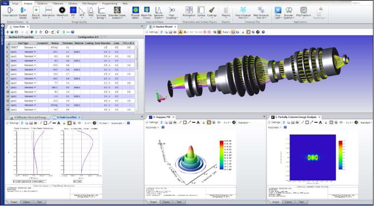
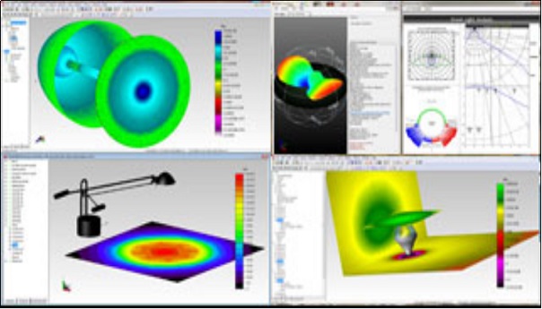
Zemax Optic Studio Refractive imagig & illumination designs & simulations |  |
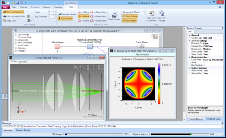
| LightTrans VirtualLab Design & optimization of diffractive beam-splitters, beam-shapers, diffusors and custom image projectors for a single wavelength light sources. |  |
 |
|  |
TracePro Design & optimization of diffractive beam-splitters, beam-shapers, diffusors and custom image projectors for a single wavelength light sources.
|  |
|
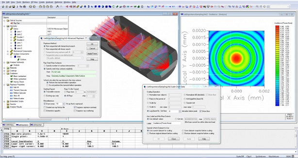
FRED Simulation of the propagation of light through any optomechanical system by raytracing |  |
 |
|  |
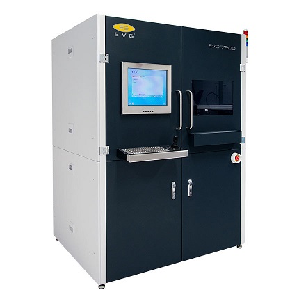
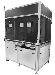
| Our Equipments EVG720 Automated SamrtNIL UV Nanoimprint Lithography System
● EVG720 with innovative SmartNIL® technology is ideally suited for high-volume manufacturing of precise micro and nano-optical elements. ● Automated full-field nanoimprint solution includes loading, imprinting, UV curing, demolding or semi-auto mode for customised operations. ● Substrate size up to Ø150mm. ● Automatic top-side alignment with repeatability accuracy of ± 3µm. |
Features
- Volume-proven imprinting technology with superior replication fidelity - Proprietary SmartNIL® technology with multiple-use polymer stamp technology - Integrated imprinting, UV curing demolding, and working stamp fabrication - Automated cassette-to-cassette handling plus semi-automated R&D mode - Optional top-side alignment - Optional mini-environment - Open platform for all commercially available imprint materials - Scalability from R&D to production - System housing for best process stability and reliability
|  |
Technical Data
|
|
|
| Parameter | Specification |
| Wafer Diameter (Substrate Size) | 75 up to 150 mm (EVG720)
75 up to 200 mm (EVG7200) |
| Resolution | ≤ 40* nm |
| Exposure Source | High-power LED (i-line) > 400 mW/cm² |
| Alignment | Optional top side alignment |
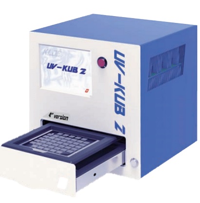
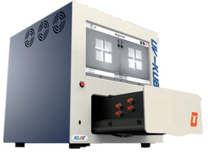
Kloé UV - KUB 2 & KUB 3
Kloé UV-Kub series is a compact tabletop masking and exposure system based on UV LED with an available light source at 365nm. The collimated system of LED-based optical heads provides a Homogeneous exposure with less than 5% variation over the substrate and enables a divergence angle below 2°. Patterns with a resolution of 2µm are possible. A wide range of lithography applications includes photolithographic processes, multilevel masking, wafer bonding, adhesive curing and wafer-level optics. Compatible with hard or soft masking contact modes with adjustable substrate distance control.
|
KUB 2 ● Exposure area up to Ø6inches substrates with mask size of 7”
| KUB 3
● Mask aligner that could achieved alignment accuracy of 2µm. ● Acceptable substrate size up to Ø4” with mask size of 5”.
|
 |  |
| Technical Data |
|
|
|
| Performances | KUB2 | KUB3 |
| Resolution | 1µm | 1µm |
| Divergence Angle | < 2° | < 2° |
| Processes | Hard (physical) or soft (proximity) contact processes | Hard (physical) or soft (proximity) contact processes |
| Wavelength | 365nm +/- 5nm | 365nm +/- 5nm |
| Working Surface | 4" or 6" wafers | 4" or 6" wafers |
| Compatible Photoresist | SU8, Shipley, AZ Resist, K-CL resist (developed by Kloe) | SU8, Shipley, AZ Resist, K-CL resist (developed by Kloe) |
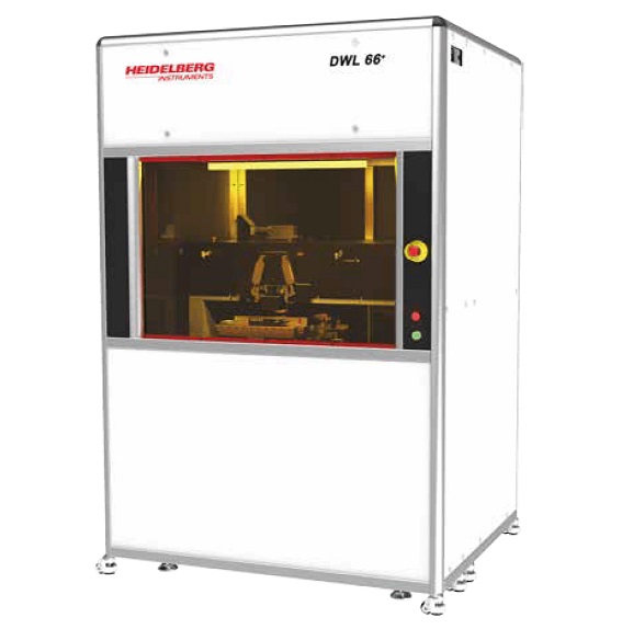
HIMT DWL66+ - The Ultimate Lithography Research Tool
● DWL66+ is a High-resolution direct laser writer and stands out with its Grayscale and Binary Exposure Modes. ● Diversity of applications such as creating complex 2.5D micro-optics, DOEs and photomask fabrication is achievable with DWL66+. ● Minimum feature sizes of 500nm and 1µm, depending on the laser write heads. ● Front- and backside alignment with 1µm overlay accuracy.
|
Features
|  |
Technical Data
|
|
|
| Write Mode | HiRes | I | II | III | IV | V |
| Writing Performance |
| Minimum Feature Size [μm] | 0.3 | 0.6 | 0.8 | 1 | 2 | 4 |
| Minimum Lines and Spaces [μm] | 0.5 | 0.8 | 1 | 1.5 | 3 | 5 |
| Address Grid [nm] | 5 | 10 | 25 | 50 | 100 | 200 |
| Edge Roughness [3σ, nm] | 50 | 50 | 70 | 80 | 110 | 160 |
| CD Uniformity [3σ, nm] | 60 | 70 | 80 | 130 | 180 | 250 |
| 2nd Layer Alignment over 5 x 5 mm2 [nm] | 250 | 250 | 250 | 250 | 350 | 500 |
| 2nd Layer Alignment over 100 x 100 mm2 [nm] | 500 | 500 | 500 | 500 | 800 | 1000 |
| Backside Alignment [nm] | 1000 |
|
|
|
|
|
| With Diode Laser (405 nm) |
|
|
|
|
|
|
| Write Speed [mm2/min] | 3 | 13 | 40 | 150 | 600 | 2000 |
| Exposure Time for 100x100 mm² area [min] | 3000 | 740 | 255 | 72 | 20 | 7 |
| With UV Diode Laser (375 nm) |
|
|
|
|
|
|
| Write Speed [mm2/min] | 2 | 10 | 30 | 110 | - | - |
| Exposure Time for 100x100 mm² area [min] | 5000 | 1015 | 350 | 100 | - | - |
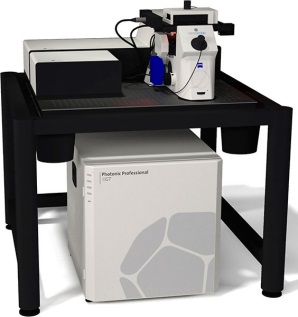
Nanoscribe Photonic Professional GT
● Photonic Professional GT employs the two-photo polymerization (2PP) 3D printing technique, ideal for research, prototyping and small-scale manufacturing dealing with sectors such as microoptics, microfluidics, photonics and micromechanics.
● Deliver optical quality surface and submicrometer resolution printing with minimum feature size of 300nm. ● Complex structures of undercuts, porous, curved, upright and smooth shapes are possible.
|
Features
- Minimum 3D lateral feature size: 300 nm (spec.); 160 nm (typ.) - Finest vertical resolution: 1500 nm (spec.); 1000 nm (typ.) - Accessible print area by motorized stage: 100 × 100 mm2 - x-y-z piezo range: 300 × 300 × 300 μm3 - x-y galvo scan range: 200–600 μm diameter (dependent on scanning objective) - Maximum object height: 3 mm (DiLL mode) - 2PP resins provided: IP-Dip, IP-L 780, IP-S - Optical-quality surfaces - Straightforward 3D printing workflow from CAD files (STL format) import to final parts - Diverse range of print materials and substrates
|  |
 | 
| 
|
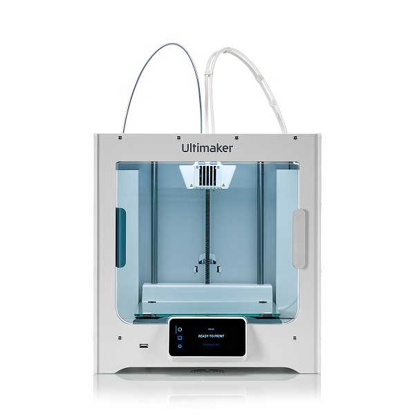
Ultimaker S3
● Ultimaker S3 is a high-quality dual extrusion 3D printer utilizes Fused filament fabrication to build functional prototypes, manufacturing and mechanical parts. ● Compatible filament materials include PLA, Nylon, PP, ABS, PC and etc, combination of materials are supported. ● Layer resolution down to 20µm with finest details are possible. ● Printable volume up to 230mm x 190mm x 200mm. |
Features
- Composite-ready dual extrusion - Advanced auto bed leveling - Aware-winning touchscreen interface - Compatible with over 110 materials
|  |
Technical Data
|
|
|
| Parameter | Spcifications |
| Layer Resolution | 0.25 mm nozzle: 150 - 60 micron
0.4 mm nozzle: 200 - 20 micron
0.6 mm nozzle: 300 - 20 micron
0.8 mm nozzle: 600 - 20 micron |
| XYZ resolution | 6.9, 6.9, 2.5 micron |
| Feeder type | Dual-geared feeder, reinforced for composite materials |
| Nozzle diameters | 0.25 mm, 0.4 mm, 0.6 mm, 0.8 mm |
| Build Speed | < 24 mm³/s |
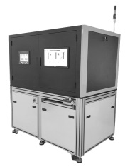
WLO Series
WLO series is well-suited for standard nanoimprint processes, perfect tool for high volume production and cost efficiency. Automated wafer handling to pickup wafer from cassette station and place it onto the imprint platform. Customized wafer chuck design according to the specific needs of customers.
|
WLO4
● Puddle dispense imprinter, feasible for both hybrid and monolithic microlens molding processes through UV-NIL. ● Equipped with highly precise top-side alignment system, reliably achieved alignment accuracy of 5um. ● Imprinting on both sides of wafer is possible. ● Substrate size up to Ø150mm.
|  |
|
|
|
WLO5
● Substrate size up to Ø150mm. ● Substrate thickness of 0.25mm to 3mm.
|  |
|
|
|
WLO6 ● Full area imprinting up to Ø200mm. ● Substrate thickness of 0.25mm to 3mm. | 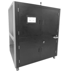 |
Contact us at info@simtrum.com for customized service.